

Samsung high performance forksheet transistor

In recent years, we have seen Samsung Foundry experience numerous setbacks in the development of its nodes. Although it was one of the first companies to introduce gate-all-around (GAA) transistor technology, it was not a complete success, and despite being one of the first to adopt EUV, Samsung ended up delaying or even skipping some nodes over the years.
Despite all the hardship, Samsung recently announced it will pursue a new strategy to narrow the technology gap with TSMC and fend off fast follower SMIC, going all-in to improve the company's advanced SF2 chip processing technology and secure more clients to compete with TSMC. Furthermore, last year, Samsung stated it plans to move to a more advanced 1.4nm-based processing technology (SF1.4 node) by 2027.
However, the reader should already know how easy it is to make bold claims in the world of technology and how difficult it can be to achieve such ambitions. It is therefore necessary to analyze the overall roadmap of the semiconductor industry and review Samsung's current research output to determine whether it is moving in the direction of surpassing its competitors or merely making empty promises.
When we carefully analyze the roadmap proposed by the semiconductor industry for the development of future process technologies and review Samsung's most recent patents, we can gain a clear idea of what Samsung's future node development path will be and whether it remains competitive in the bloody race for leading-edge semiconductors.
Paving the way for Forksheet
In recent years, not only Samsung but also other manufacturers have been migrating to nanosheet-based GAA transistors, an elegant solution for continuing the transistor scaling process. This approach compensates for the degradation of the drive current and offers both enhanced electrostatic control and a reduced footprint compared to FinFET.
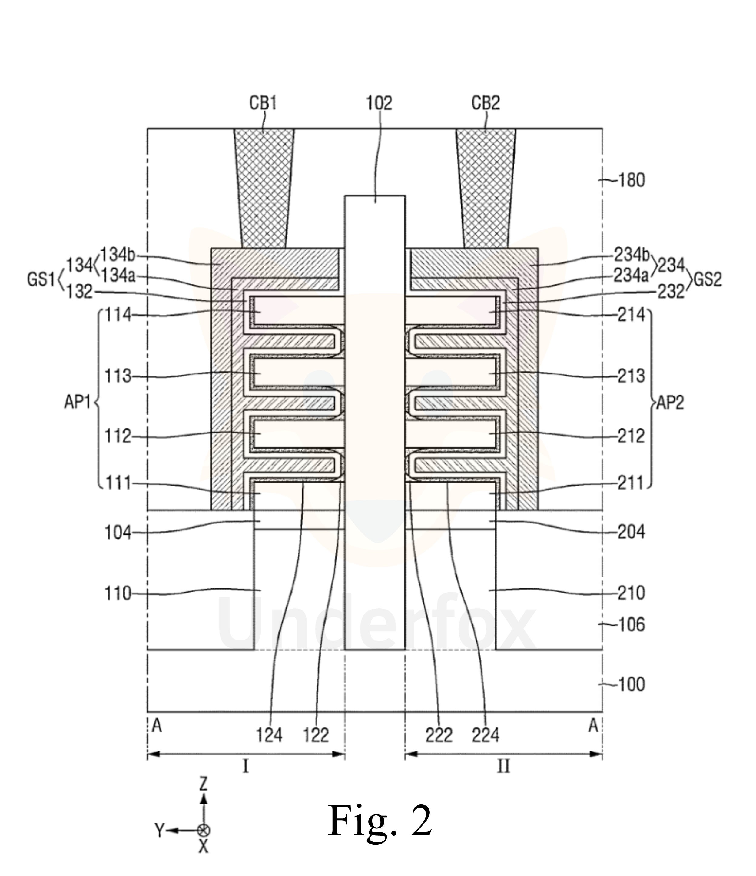
However, the next step in the evolution path before entering the era of picometers—with the emergence of CFET—would be Forksheet transistors. In this evolutionary step, a dielectric wall is introduced between the nMOS and pMOS devices, with hardmask patterning for the work function metal now performed on this dielectric wall rather than at the bottom of the gate trench, as is the case with nanosheets, allowing for much tighter n-to-p spacing.
Until recently, only Intel, TSMC, and Imec had shown real progress in developing and improving the proposal for this new type of device (Stacked Forksheet from Intel). However, everything changed in recent months with two patent applications filed by Samsung that clearly demonstrate its intention to advance rapidly in the development of Forksheet transistors.
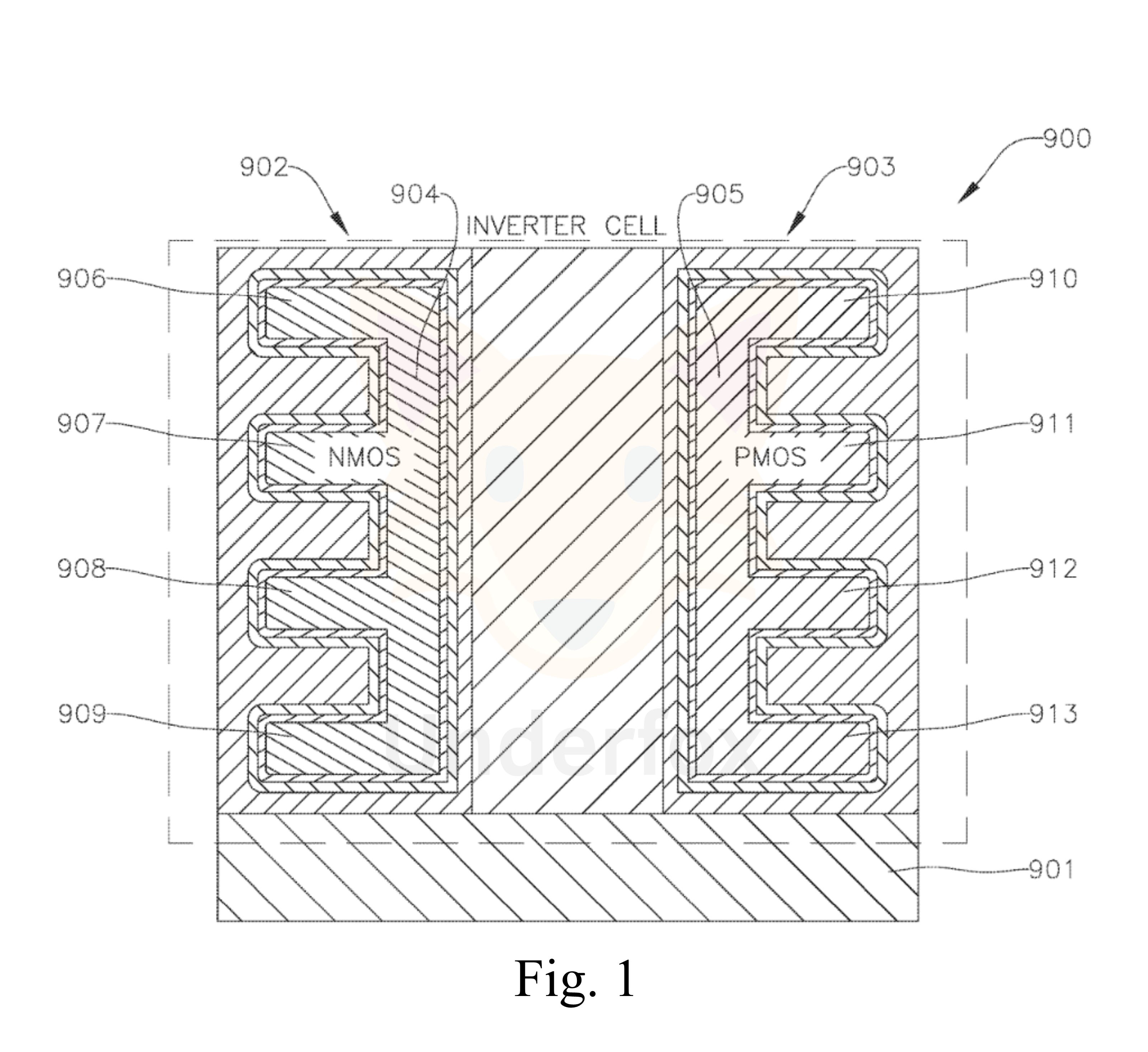
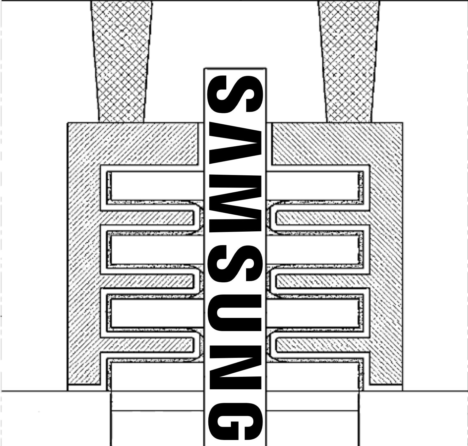
In early December, Samsung published a patent application for a high-performance forksheet transistor which is configured to increase drive current by approximately 31% when compared to a forksheet node having the same area footprint, and achieve up to approximately 17% area scaling when compared to a GAAFET (In this case, SF3).
Furthermore, the patent highlights several measurements that provide a general idea of the formation of the standard cell. For example, the stem has a width of approximately 4–6 nm and a height of approximately 45–55 nm; each prong has a width of approximately 10–20 nm and a height of approximately 4–6 nm; adjacent prongs are spaced apart in the vertical direction by approximately 10–15 nm; and the dielectric wall has a width of approximately 15–20 nm.
When we compare the numbers presented in the patent with the works published to date by Imec, we gain a clear idea of the progress Samsung has achieved so far in the development of Forksheet transistors, which will undoubtedly form the foundation of its cutting-edge nodes in the future. And it doesn’t stop there…
2D channel layer on the way
To further improve the scaling process and electrostatic control in Forksheet transistors, Samsung researchers have proposed, in a second patent application published a few days ago, the addition of 2D channel layers to the transistor structure to enhance mobility and significantly reduce the short-channel effect. The 2D channel layer is formed from a transition metal dichalcogenide, which may be molybdenum disulfide (MoS₂) or tungsten disulfide (WS₂), as suggested in the patent.
Although the patent is vague regarding the process of growing this 2D channel layer and the current progress of related research, focusing instead on describing the method's application, it clearly demonstrates at least an interest in further improving the scaling process of its Forksheet transistors.
The reader must understand that the method proposed in this patent for enhancing mobility and mitigating the short-channel effect through the use of two-dimensional semiconductor material as a channel is still an open field of study, with many challenges yet to be overcome. What can be said for now is that this patent indicates Samsung is genuinely interested in advancing its roadmap toward the development of 2D transistors, which would undoubtedly include CFETs with 2D channels.
The bloody race continues
The struggle in the development of process technology has become a bloody race over the past 20 years. It doesn’t take much argument to see that the challenges facing the semiconductor industry are unprecedented. The number of companies with integrated fabrication facilities at the process frontier has dwindled, dropping from 29 in 2001 to 8 by 2015.

This number has only worsened in recent years, with only three companies currently leading the development of new leading-edge nodes. This is a worrying trend that potentially threatens global economic growth, making collective research and development efforts and government incentives necessary to change this scenario.
Therefore, it is with great joy and hope that I observe Samsung's decisions, amidst such difficulties and setbacks in its latest nodes, to persevere in the research and development of Forksheet transistors. As Imec has rightly stated, Forksheet is a necessary intermediate step toward achieving several key milestones on the path to CFETs. By continuing to pursue the development of advanced nodes, Samsung demonstrates that it remains a competitor in this fierce race for leading-edge processes. And the Forksheet race is on.
Some references and further reading:
Hassan N. Khan, David A. Hounshell, E. Fuchs, Science and research policy at the end of Moore’s law, Nature Electronics volume 1, pages 14–21 (2018) [Link]
M. Liu, J. Niu, G. Yang, K. Chen, W. Lu, F. Liao, C.n Lu, N. Lu, L. Li, Large-Scale Ultrathin Channel Nanosheet-Stacked CFET Based on CVD 1L MoS2/WSe2, Advanced Electronic Materials Volume 9, Issue 2, (2023) [Link]
US20240405128 - Field effect transistor (FET) and method of manufacturing the same - Kumar et al. - Samsung [Link]
US20240413251 - Semiconductor device and method for fabricating the same - Lee et al.- Samsung [Link]
US20240321961 - Integrated circuit device - Kim et al. - Samsung [Link]
Changelog
v1.0 - initial release;
Donations
Monero address: 83VkjZk6LEsTxMKGJyAPPaSLVEfHQcVuJQk65MSZ6WpJ5Adqc6zgDuBiHAnw4YdLaBHEX1P9Pn4SQ67bFhhrTykh1oFQwBQ
Ethereum address: 0x32ACeF70521C76f21A3A4dA3b396D34a232bC283