

Intel graphics odyssey Pt. 2 – The quest for the chiplet way

In recent years, multi-chiplet GPU designs have become more and more attractive as monolithic GPUs are reaching the reticle limit, and it's becoming ever clearer that Moore's Law has its days numbered. However, there are several problems in determining how to disaggregate a GPU into multiple processor blocks.
First, GPU data traffic has a very different pattern from CPUs, having a many-to-few-to-many traffic pattern around the memory controllers, which generates traffic bottlenecks. Second, while including a large number of blocks in a GPU can bring significant benefits, it can also increase the level of complexity in NoC routing with the addition of each block at an exponential level. Finally, one should also consider the power management issues of a multi-chiplet GPU. If powering all blocks during operation can result in excessive energy consumption, in some cases much greater than the equivalent monolithic design, on the other hand, it is also highly complex to try to manage the energy consumption of each block separately.
Such design choices are of crucial importance because they directly affect the scaling performance of a multi-chiplet GPU. All these choices are part of the great odyssey that Intel Graphics has challenged itself to face. So, before we delve into a deeper discussion of the technical details of what Intel plans for its next-gen GPUs, it would be convenient to know how Intel will address these challenges. When we look closely at their latest patents, we can get an idea of how Intel will solve their quest.
How to make a mosaic


A recently published patent presents some of Intel's views on how it plans to solve the design problems of its future multi-chiplet GPUs, as well as clearly showing how their design proposal will evolve in the generations to come. The patent clarifies Intel's intention to use multiple chiplets in its future GPU designs, using serial or parallel links to interconnect them, as well as applying signal compression to reduce the overhead involved in communicating between its multiple blocks.
Additionally, the patent also suggests the use of architectural sharing of physical pins or wires between blocks to reduce the cost and complexity of fabrication, potentially reducing the overall physical size of the GPU design. To facilitate the control of GPU scaling, the use of a subcluster architecture will be applied, where each subcluster can have a variable number of blocks and where each of the blocks in the subcluster can have different functions.
All these design approaches described above can be found in Ponte Vecchio, and these will be the foundations of all Intel multi-chiplet GPU architectures in the coming years, both for gaming and HPC solutions. However, the patent goes even deeper, showing how Intel plans to apply a disruptive and heterogeneous approach to maximize GPU chiplet utilization.
Asymmetrical multi-chiplet GPU architecture


In a conventional multi-chiplet GPU architecture design, it is common, for reasons of simplicity, to subdivide the GPU into a few homogeneous functional blocks. However, the use of an asymmetric architecture can bring several benefits, both in manufacturing and in overall GPU performance. Thus, Intel proposed in its patent the construction of an asymmetric GPU architecture, using chiplets of different sizes and specific functions in order to maximize its die recovery plan and opportunistically improve chip utilization in its GPU architecture.
In terms of the manufacturing process, the patent proposes using functional blocks of varying sizes in such a way that larger blocks have more resources than smaller ones. Furthermore, such blocks may contain different hardware units and may have part of their operational functions fused off and not available, as in the case of die recovery where part of the block is defective and has been deactivated. The patent itself cites, as an example, tensor processing units being decoupled from vector processing units, or raster/texture processing units being decoupled from processors. It is important for the reader to understand that the use of fusing is not limited exclusively to defective dies; it can also be applied to other chiplets to achieve certain desired characteristics for the chiplets on the GPU. In addition, the patent places great emphasis on the fact that the chips do not need to have a perfectly rectangular shape but can assume any shape without any difference in their final functionality. It is very important to emphasize this observation, as it is possible that there are products with different chip formats and different numbers of chips, which can lead to some confusion when other technology analysts disassemble their GPU samples.


In terms of architectural design, the patent proposes that different blocks can be built to support different ISAs. The initial example provided by the patent would be a composite-ISA architecture, formed by the combination of blocks with single and double precision format support. However, we can go further by exploring other patents, such as the inclusion of a micro-FPGA chiplet, formed by adaptive logic modules (ALMs) capable of being programmed to accelerate ray tracing and deep learning on its GPUs, thus creating a more definitive heterogeneous gaming solution. All these blocks are designed to provide different performance characteristics in order to allow the selection of a specific block for a specific workload by the hardware scheduler, thus allowing for a tradeoff of performance and power. It is important for the reader to note that many current GPU workloads are non-uniform, having multiple wavefronts with predicate-off threads. Such instructions still take up significant space in the pipeline, making even homogeneous multi-chiplet GPUs energy inefficient. Therefore, by providing a set of execution resources within each GPU chiplet tailored to a range of execution profiles, this proposed asymmetric GPU architecture can better handle irregular workloads in a more efficient way.
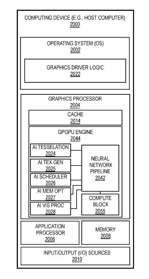
It is important to remember that the first part of this article presented a detailed breakdown of the Intel AI GPGPU architecture. Now, with the information provided by this new patent application, it is possible to see more clearly how the implementation of the new AI GPGPU pipeline proposal will be integrated with the conventional pipeline by adding multiple neural blocks to its composition.


Finally, considering the significant differentiation proposed between the chiplets that comprise the multiple functions of the GPU, Intel will implement a method of dynamically assigning cores exclusively to fixed function units. This approach aims to increase flexibility for the system by allowing a mix-and-match of resource trade-offs to achieve specific optimal power and performance characteristics in the GPU. Based on the performance scalability ratio, which relates the workload power/performance scalability among the fixed functions, it is possible that a particular fixed function unit may offer fast performance but be costly in terms of power usage, while another fixed function unit may be more functional but slower in operation and consume less power. Therefore, the implementation of a process for the dynamic exclusive assignment of cores to fixed function units, enabling symmetric or asymmetric ISA support for processing when necessary to meet the power requirements of the GPU, will lead, over time, to a substantial improvement in GPU energy efficiency.
The Intel chiplet quest
Adopting a chiplet-based architecture is definitely not an easy task. There are several choices and trade-offs that Intel will have to make in its search for a development path for its new architectures. Throughout this silicon journey, there is already a predetermined fact: There will be no future for anyone waiting for a Deus Ex Machina1 to happen.
The widespread use of chiplets, already foreseen by Moore himself, is the last breath of his Law before the ultimate end. However, even in these final moments, a huge research effort will still be needed to develop solutions that allow a greater level of system disaggregation so that such multi-chiplet architectures can effectively bring an increase in computing power to the world.
Intel is putting a lot of effort into the development of its new GPUs, and many of the design choices it is making have great potential to move Intel into a leadership position in GPU technology development. In the end, while Intel bravely goes through the long and arduous journey of its odyssey, Nvidia has been on its Sisyphean task for years, trying again and again to solve its monolithic problems, which are growing ever larger, by the way.
Some references and further reading:
US20220107914 - Multi-tile architecture for graphics operations - Koker et al. - Intel [Link]
US10929134 - Execution unit accelerator - Sripada et al. - Intel [Link]
US11151769 - Graphics architecture including a neural network pipeline – Labbe et al. – Intel [Link]
Underfox – “Intel Graphics Odyssey Pt. 1 – The AI GPGPU is a game changer” – Coreteks – 2020 [Link]
Underfox – “The Alder Lake hardware scheduler – A brief overview” – Coreteks – 2021 [Link]
Changelog
v1.0 - initial release [Link];
v1.1 - Added some captions to improve accessibility and fix special thanks;
v1.2 - (current) Some spelling corrections and small changes to improve clarity;
A direct reference to Professor Michael B. Taylor and his article "Is Dark Silicon Useful? Harnessing the Four Horsemen of the Coming Dark Silicon Apocalypse" presented at the Design Automation Conference, June 2012.