The Intel Valleytronic MESO overview
In 2015, Intel researchers published the first preprint of a promising, viable beyond-CMOS logic technology: the MESO device—a scalable spintronic logic device that operates via spin-orbit transduction combined with magnetoelectric switching, which converts an input voltage/charge into a magnetic spin state (e.g., charge-to-spin conversion) and uses spin-orbit transduction to convert the magnetic spin state into an output charge/voltage (e.g., spin-to-charge conversion). In this form, the initially proposed spintronic device could enable continued scaling of logic performance close to thermodynamic limits, offering higher integration density and efficiency while being non-volatile, which counteracts leakage power and enables ultra-low standby power.
However, there was a significant issue associated with the MESO logic design that made it unfeasible as a direct replacement for CMOS logic: ensuring that the output signal of one MESO device is large enough to drive the input of other MESO devices. In fact, the output power of a MESO device depends on the efficiency of the spin-to-charge conversion readout, which has been a limiting factor for building higher-order majority gates. During the spin-to-charge conversion, most spins dissipate at the interface of the spin-orbit module and the magnet due to scattering, conductance mismatch, and lattice mismatch, which dramatically reduces the output signal.
To address this issue, Intel researchers recently proposed a new approach to the MESO device that, combined with other recent developments, could once again allow Intel to reach a new milestone in semiconductor history.
The valleytronic approach
In early July, a new Intel patent application was published, proposing a design based on valleytronics, which explores the valleys in the electronic band structure. The patent proposes the use of a new 2D valleytronic layer in its spin-to-charge conversion output module, thus transforming the device into a valleytronic MESO.


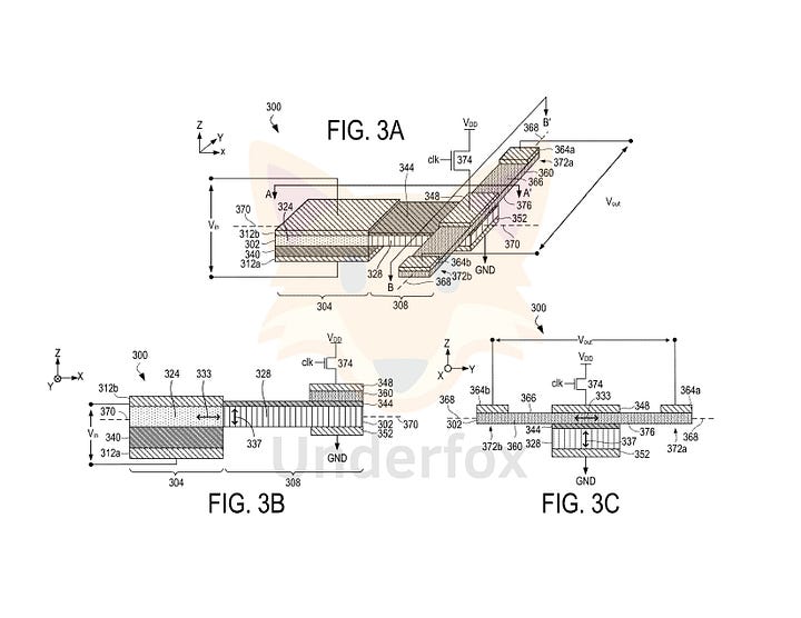
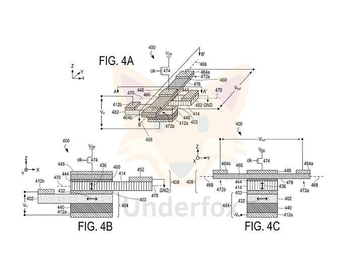
The charge-to-spin conversion input module and the spin-to-charge conversion output module share a ferromagnet, with the input module comprising a ferromagnet with in-plane magnetic anisotropy (IMA) and the output module comprising a ferromagnet with perpendicular magnetic anisotropy (PMA). The PMA ferromagnet is used to inject spin-polarized current into the 2D valleytronic layer, which converts the spin-polarized current into an output charge current via the inverse spin Hall effect.
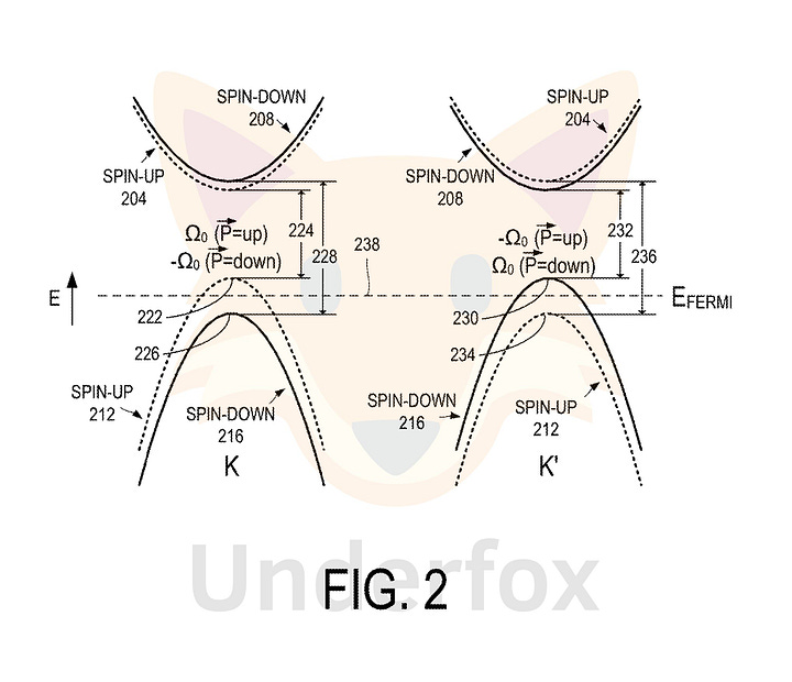
The valleytronic MESO device utilizes band spin-splitting to read out the device's logic state, which is stored as the magnetization orientation of the IMA and PMA ferromagnets. Chiral coupling between the IMA and PMA ferromagnets through antisymmetric exchange causes the perpendicular magnetization orientation of the PMA ferromagnet to switch with the magnetization orientation of the IMA ferromagnet. If the spin current injected from the PMA ferromagnet into the 2D valleytronic layer is spin-up polarized, the 2D valleytronic layer will predominantly comprise spin-up electrons in the valley where the valence sub-band for spin-up electrons is closest to the Fermi energy level and has a positive Berry curvature. Similarly, if the injected spin current is spin-down polarized, the valleytronic layer will predominantly comprise spin-down electrons in the valley where the valence sub-band for spin-down electrons is closest to the Fermi level and has a negative Berry curvature.
The geometry of the device proposed in the patent is significantly altered from the original MESO proposal, having a cross-shaped geometry, in which the 2D valleytronic layer is substantially orthogonal to the PMA ferromagnet. The spin-polarized charge current injected into the 2D valleytronic layer is converted into a differential voltage output across the 2D valleytronic layer via the inverse spin-valley Hall effect, whereby charge carriers acquire an anomalous velocity proportional to the Berry curvature and an applied electric field. The anomalous velocity is along the direction of an axis that extends the length of the 2D valleytronic layer.
Among the many advantages of this new MESO design, the main and most important one is that the PMA ferromagnet in the spin-to-charge conversion output module allows for the injection of out-of-plane spin current into a valleytronic monolayer that has a strong valley-coupled spin Hall effect. Thus, the proposed valleytronic spin-to-charge conversion output module has a larger output current/voltage than is possible in MESO devices with a traditional spin-to-charge output module, allowing one valleytronic MESO device to have energy enough to drive the input of other MESO devices. Furthermore, the new spin-to-charge conversion output module has a simpler stack design than the traditional MESO design, which is better for scaling purposes.
The final roadmap
On average, it takes around 12 years for an emerging technology to reach consumers. The entire semiconductor industry is working to accelerate the development of spintronics and valleytronics, and Intel is no exception.
Intel has proposed an ambitious timeline of 2025 for this technology to reach its processors. With the arrival of Pat Gelsinger as CEO, Intel has gotten back on track with respect to executing a viable roadmap. Intel's 18A node has shown significant advancements, along with notable progress in 2D TMD channel materials.
At VLSI 2024, Intel presented a unique gate oxide atomic layer deposition process and a low-temperature gate cleaning process to build GAA devices that demonstrated breakthrough performance for MoS2- and WSe2-based GAA NMOS and PMOS transistors. But as important as the results presented are the methods developed to achieve them. New patent applications for methods of fabricating devices using ion beams, creating precision defects in TMDs, as well as the new technique proposed to form RibbonFETs with multiple single-grain TMD channels, clearly show that Intel is making great strides toward making it feasible to manufacture such innovative devices as this new valleytronic MESO proposal.
I might be inclined to feel a bit optimistic about Intel achieving their ambitious goal. For now, all the results shared here indicate that Intel researchers are working pretty hard to make this vision a reality on time—something I haven’t seen in quite a while.
Some references and further reading:
US20240224814 - Chiral coupling-based valleytronic magnetoelectric spin-orbit devices - Debashis et al. - Intel [Link]
Michael Berger - Valleytronics explained - Nanowerk (2023) [Link]
US20240222126 - Fabrication of novel devices using ion beams - Kavrik et al. - Intel [Link]
US20240222428 - Seeded Growth For 2D Nanoribbon Transistors - Dorow et al. - Intel [Link]
S. Manipatruni, D. E. Nikonov, R. Ramesh, H, Li, I. A. Young, Spin-Orbit Logic with Magnetoelectric Nodes: A Scalable Charge Mediated Nonvolatile Spintronic Logic, Arxiv (2015) [Link]
Changelog
v1.0 - initial release;
Donations
Monero address: 83VkjZk6LEsTxMKGJyAPPaSLVEfHQcVuJQk65MSZ6WpJ5Adqc6zgDuBiHAnw4YdLaBHEX1P9Pn4SQ67bFhhrTykh1oFQwBQ
Ethereum address: 0x32ACeF70521C76f21A3A4dA3b396D34a232bC283


